The transmission rate of high-speed PCB design and routing system is accelerating with the changes of the times, but which also brings a new challenge to it – The anti-interference ability is getting weaker and weaker. This all stems from the fact that the higher the frequency of information transmission, the more sensitive the signal and the weaker the energy, so the routing system is more and more susceptible to interference. In some common electronic equipment, such as computer screens, mobile phones, motors, radio broadcasting equipment, etc., cables and equipment are able to interfere with other components or be seriously interfered by other interference sources.
Shielding Methods In High Frequency PCB Design
Especially when using high-speed data networks, the time required to intercept a large amount of information is significantly lower than the time required to intercept low-speed data transmissions. The twisted pair in the data twisted pair can resist external interference and inter-pair crosstalk through its own twisting at low frequencies, but at high frequencies (especially when the frequency exceeds 250MHz), the twisting alone cannot achieve anti-interference. Purpose, only shielding can resist external interference.
The cable shield acts like a Faraday shield. Interfering signals enter the shield, but not the conductors. Therefore, the data transfer can operate without problems. Network transmission is blocked because shielded cables have lower radiated emissions than unshielded cables. Shielded networks (shielded cables and components) can significantly reduce the radiation level of electromagnetic energy that may be intercepted as it enters the surrounding environment.
Shielding options for different interference fields mainly include electromagnetic interference and radio frequency interference. Electromagnetic interference (EMI) is mainly low frequency interference. Electric motors, fluorescent lamps, and power lines are common sources of EMI. Radio frequency interference (RFI) refers to radio frequency interference, mainly high frequency interference. Wireless communications such as radio, television broadcasting, and radar are common sources of RF interference. For immunity to EMI, braided shielding is the most effective because of its lower critical resistance; For RFI, foil shielding is the most effective. Since the braided shielding depends on the change of wavelength, the gap generated by the braided shield allows the high-frequency signal to freely enter and exit the conductor; for the mixed interference field of high and low frequencies, the combined shielding method of the foil layer with the broadband coverage function and the braided mesh should be adopted. Generally speaking, the higher the mesh shielding coverage, the better the shielding effect.
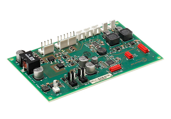
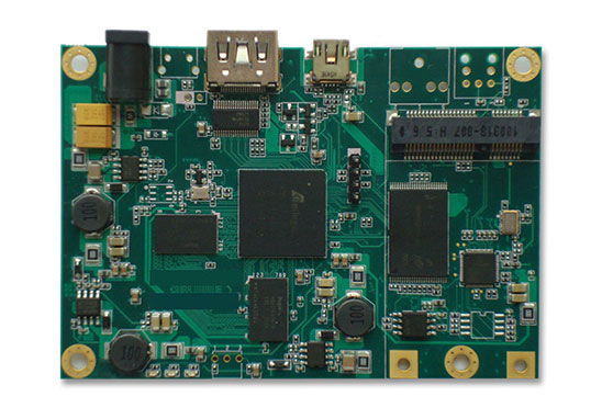
Grande’s PCB Design Capabilities
Maximum Signal Design Rate: 10Gbps CML differential signal; Maximum PCB Layout Layers: 40 layers; Minimum Line Width: 2.4mil; Minimum Line Spacing: 2.4mil; Minimum BGA PIN Spacing: 0.4mm; Minimum Mechanical Hole Diameter: 6mil; Minimum Laser Drilling Diameter: 4mil; Maximum Number of PINs: ;63000+ Maximum Number of Components: 3600; Maximum Number of BGAs: 48+.
Advantages Grande Circuit Board Assembly
1)Strength Guarantee
▪ SMT factory: With imported SMT machines and multiple optical inspection equipment, which is able to produce 4 million points per day. Each process is equipped with QC personnel who will keep an eye on product quality.
▪ DIP production line: Two wave soldering machines and more than 10 employees who have worked for over three years. That’ s to say, these workers are highly skilled and can weld various SMT & DIP components.
2)Quality Assurance With High Cost Performance
▪ High-end equipment can paste precision special-shaped parts, BGA, QFN, 0201 package. It can also be soldered prototype PCBA via SMT machine and placing bulk materials by hand.
▪ Both samples, small and large batches can be produced. And there is no SMT Machine starting cost.
3)Rich Electronic Products SMT Soldering Experience With Stable Delivery
▪ Accumulated services to thousands of electronics companies, involving SMT soldering services for various types of automotive equipment and industrial control motherboards. Furthermore, PCBA Products are often exported to Europe and the United States, and the quality is able to be affirmed by new and regular customers.
4)Strong Maintenance Ability & Reliable After-Sales Service
▪ The maintenance engineers have sophisticated experience so that those defective boards caused by all kinds of SMT soldering can be repaired. Meanwhile, ensuring the connectivity rate of each circuit board also make sense.
▪Order problems feedback will get response, solution and solved as soon as possible.
The rapid development of science and technology determines that all enterprises must improve accordingly. Among them, PCBs depend on technology and naturally must not fall behind. Therefore, the layout of high-frequency PCBs has become a key point that everyone need to discuss when designing high-frequency PCBs. Then what are the attention points in high-frequency PCB Design?
Attention Points In High Frequency PCB Design
(1) High-frequency circuits tend to have high integration and high-density PCB design routing. Therefore, the use of multi-layer boards is both necessary for PCB design routing as well as an effective means of reducing interference.
(2) The less the lead bends between the pins of the high-speed circuit device, the better. The lead wire of the high-frequency circuit PCB design and routing is preferably a solid line, which need to be wound, and can be folded with a 45° folded line or an arc. To meet this requirement, external transmission and mutual coupling of high-frequency signals can be reduced.
(3) The shorter the lead between the pins of the high-frequency circuit device, the better.
(4) The alternating between the trace layers between the pins of the high-frequency circuit device should be as small as possible. The so-called “minimize interlayer crossover” means that the fewer vias used in the component connection process, the better. It is estimated that one via can bring about 0.5 pF of distributed capacitance. Reduced the number of vias is able to greatly increase the speed.
(5) High-frequency circuit PCB design and layout should pay attention to the “cross-interference” introduced by the parallel traces of the signal traces. If parallel distribution cannot be avoided, a large area “ground” can be placed on the back of the parallel signal traces to greatly reduce interference. Parallel traces in the same layer are almost inevitable, but in two adjacent layers, the traces must be oriented perpendicular to each other.
(6) Grounding measures surrounding particularly important signal traces or local units, that is, drawing the outer contour of the selected object. Using this feature, so-called “packet” processing can be performed automatically on selected important signal traces. Of course, for high-speed systems, it is also very beneficial to use this capability for local processing of components such as clocks.
(7) Various types of signal traces cannot form loops, and ground wires cannot form current loops.
(8) A high frequency decoupling capacitor should be placed near each IC block.
(9) A high frequency turbulent link should be used when connecting the analog ground trace and the digital ground trace to the common ground trace. In the actual assembly of high frequency turbulent chains, high frequency ferrite beads passing through the central hole are often used and are often not represented in circuit schematics and the resulting netlist does not include such components, the PCB design routing will Ignore its existence. Responding to this reality, it can be used as an inductor in the schematic, and the component footprint is individually defined in the PCB Component Library and manually moved to a suitable location near the convergence point of the common ground traces before routing the PCB design.
(10) Analog circuits and digital circuits should be arranged separately. After the independent PCB design is routed, the power and ground traces should be connected at one point to avoid mutual interference.
(11) Before connecting the DSP off-chip program memory and data memory to the power supply, filter capacitors should be added and placed as close as possible to the chip power pins to filter out power supply noise. Also, shielding around the DSP and off-chip program memory and data memory is recommended to reduce external interference.
(12) The off-chip program memory and data memory should be placed as close to the DSP chip as possible. At the same time, the layout should be reasonable so that the lengths of the data lines and address lines are basically the same, especially when there are multiple memories in the system, the clock traces of each memory should be considered. The clock inputs are equally spaced, or a separate programmable clock driver chip can be added.
For the DSP system, the external memory with the same access speed as the DSP should be selected, otherwise the high-speed processing capability of the DSP will not be fully utilized. The DSP instruction cycle is nanoseconds, so the most common problem in DSP hardware systems is high frequency interference. Therefore, when making the printed circuit board (PCB)of the DSP hardware system, special attention should be paid to the address lines and data lines. The routing of the signal trace should be correct and reasonable. When routing, try to keep high-frequency traces short and thick, and keep away from signal traces that are prone to interference, such as analog signal traces. When the circuits around the DSP are more complex, it is recommended to combine the DSP and its clock circuit, reset circuit, off-chip program memory and data memory into a minimal system to reduce interference.
The above is an introduction to the key points of high-frequency PCB design and layout. Grande is a PCB design company specializing in electronic product circuit board layout, which mainly undertakes multi-layer, high-density PCB layout & board prototype business. The PCB layout team with an average of more than 10 years of work experience can proficiently use the mainstream PCB design software in the market, professional and efficient communication to ensure the progress of the PCB design, and help you seize the market opportunities earlier!
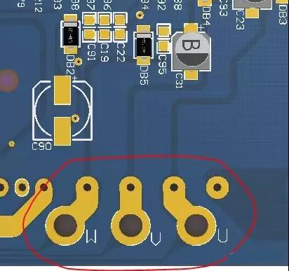
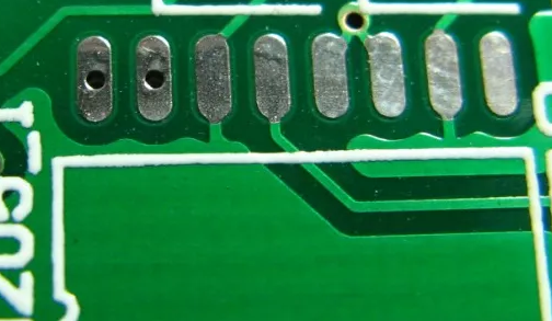
Generally, the leads on the PCB are covered with solder mask to prevent short circuits and equipment damage. The so-called solder mask opening is to remove the solder mask layer on the wire so that the wire can be exposed to tin.
What’s The Purpose of Solder Mask Opening in PCB Design?
Solder Mask Openingin PCB design can not only realize the PCB as a plug-and-play plug-in, but also increase the thickness of the solder to achieve the purpose of allowing high current.
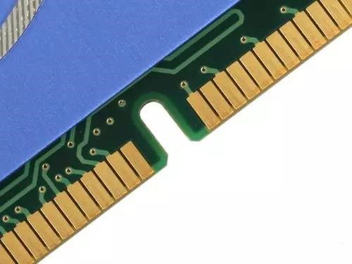
As shown in the figure above, solder mask opening. It is common for PCBs to design as solder mask opening, and the most typical one may be a memory stick. Anyone who takes apart the computer knows that there is a gold finger on the memory stick, as shown in the figure below:
In this case, gold finger is design as solder mask opening, plug and play.
Apart from that, solder mask opening also has a ordinary function, that is, the later iron increases the thickness of the copper foil, which is convenient for heavy current, which is widely used on the power supply board and the motor control board.
How can we design solder mask opening?
In PCB Design, threading and opening can be set on the TOP/BOTTOM SOLDER Layer.
TOP/BOTTOM SOLDER : It is applied to prevent tin on the copper foil and maintain insulation.
Therefore, solder mask opening is able to set on this layer to the pads, vias and non-electrical traces of this layer.
1. In PCB design, the solder pad will be opened by default (OVERRIDE: 0.1016mm), that is, the solder pad exposes the copper foil, expands by 0.1016mm, and solder is applied during the wave soldering process. It is recommended not to make any design changes to ensure solderability;
2. In the PCB design, the vias will be opened by default (OVERRIDE: 0.1016mm), that is, the via has exposed copper foil, expanded by 0.1016mm, and has wave soldering tin. If the design is to prevent SOLDER from pasting on SOLDER MASK, you must select the PENTING option of SOLDER MASK to close SOLDER MASK.
3. In addition, non-electrical wiring can also be carried out separately in this layer, so that the solder mask can be blocked and be opened accordingly. If it is on a copper foil wire, it is used to enhance the ability of the wire to heavy current. Tin is added during the soldering process. If you use non-copper wire, usually used for logo and special character screen printing, you can omit it to create a character screen layer.
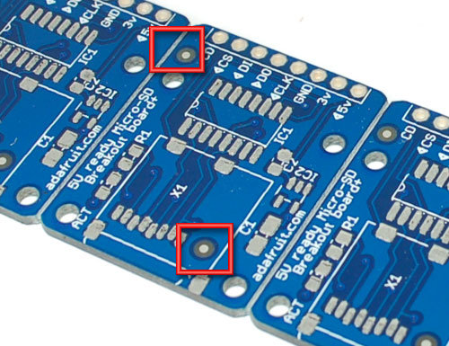
In order to facilitate the assembly of the printed circuit board (PCBA), fiducial mark will be designed on the PCB board. Do you konw? The requirements and specifications of fiducial mark In PCB Design?
What Is PCB Fiducial Mark?
Circuit board fiducial mark refers to determining the specific position of the PCB via in the PCB design process, which is a super important link in the PCB design process. After all, the function of the fiducial mark is the processing benchmark when the printed circuit board is maufactuered. There are various positioning methods for PCB fiducial mark, mainly in the light of different positioning accuracy requirements. The fiducial mark on the printed circuit board should be represented by special graphic symbols. When the requirements are not high, larger mounting holes in the printed circuit board can also be used instead.
In order to facilitate the fixing of the board during drilling and milling of the printed circuit board, as well as to facilitate online testing, plenty of circuit board manufacturers want users to design three non-metallized holes on the PCB. And the fiducial mark is usually designed as non-metallized holes, and the drilling diameter unit is basically mm. If the board surface is tight, at least two fiducial marks should be placed and placed diagonally. If you want to produce panel board, you can also regard the whole panel board as a PCB, and the entire panel board only need fiducial marks. If the user does not place it, the circuit board manufacturer will automatically add it without affecting the circuit, or use the existing non-metallized holes in the board as fiducial marks.
Positioning Fiducial Mark Method
Device hole interface devices and connectors are mostly plug-in components. The diameter of the through hole of the plug-in device is 8 to 20 mil larger than the diameter of the pin, and the tin penetration is good when soldering. It should be noted that there is an error in the aperture of the circuit board factory. The approximate error is ±0.05mm. Every 0.05mm is a drill. The diameter is more than 3.20mm, and every 0.1mm is a drill. Therefore, when designing the aperture of the device, the unit should be converted into millimeters, and the aperture should be designed to be an integer multiple of 0.05. The plate manufacturer sets the size of the drilling tool according to the drilling data provided by the user. The size of the drilling tool is usually 0.1-0.15mm larger than the forming hole required by the user. Less is better. If it is a crimping device, the aperture should not be enlarged, it should be designed according to the recommendations of the data, and which are the crimping devices should be explained in the board making instructions, so that the circuit board manufacturer can try to control the error during the board making process and avoid some unnecessary trouble.
PCB Design Fiducial Mark Requirements & Specifications
Drilling types are divided into metallized holes and non-metallized holes. There is copper sinking in the hole wall of the metallized hole, which can play a conductive role and is represented by PTH. There is no copper sinking in the hole wall of the non-metallized hole, which can not play a conductive role, which is represented by NPTH. The difference between the outer diameter and the inner diameter of the metallized hole diameter should be greater than 20mil, otherwise the soldering ring of the pad is too small to be processed, and it is not conducive to soldering. If conditions permit, the aperture can be designed to be the radius of the pad. The maximum drilling diameter of metallized holes is 6.35mm, and the maximum drilling diameter of non-metallized holes is 6.5mm. The metallized hole should not be designed on the outline, and the edge of the hole should generally be greater than 1mm from the outline. Heavy holes while drilling are easily able to damage the drill bit, so it should be avoided as much as possible. Holes that do not require soldering and have no electrical characteristics can be designed as non-metallized holes. Non-metallized holes do not need to be designed with pads. The edge of the hole is at least 1mmo away from the circuit or copper foil. Drilling can be divided into circular holes and rectangular holes according to the shape. Most of the drilled holes are round holes, and rectangular holes are drilled multiple times by the drill bit according to the prescribed procedure. Therefore, it is best to design the rectangular hole to be twice as long as the width, and the width is not less than 0.8mm, and the rectangular hole should be designed as little as possible.
PCB Fiducial Mark Requirements
The development of the PCB design industry has become mature, so the requirements for PCB fiducial marks are also rather perfect. The fiducial mark requirements are as follows:
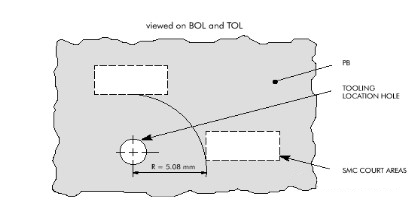
1. At least two fiducial marks must be set on the diagonal of the board. 2. The standard diameter of the fiducial mark is 3.2mm_+0.05mm. 3. The following preferred apertures can also be used for the veneer of different products of the enterprise: 2.8mm±0.05mm, 3.0mm±0.5mm, 3.5mm±0.5mm and 4.5mm±05mm. For different boards of the same product (such as the DT board and PP board of ZXJ10), if the external dimensions of the PCB are the same, the positions of the positioning holes must also be unified. 4. The fiducial mark is a light hole, that is, a non-metallized through hole (except for the RF board). 5. If the existing installation holes (except the buckle installation holes) meet the above requirements, there is no need to set additional fiducial marks.
Some Common Specifications & Accuracy Requirements For Fiducial Marks
1. The diameter error range of the fiducial mark is generally within 0.01mm. If the PCB manufacturing room has a large error, it will cause poor contact of the probe and inaccurate alignment of the interface connector automatic mechanism. 2. Requirements for the diameter of the fiducial mark: Try to be below 3mm, so that the positioning column will not be deformed, and it is not easy to operate if it is too large. 3. The distance between the fiducial mark and the PCB network: More than 1MM, so that the installation operation is not easy to short-circuit, and it will not cause damage to the product line. 4. Type of fiducial mark: The fiducial mark is generally a mechanical control that requires no copper sinking, so that it is not connected to the circuit on the board and has higher precision. 5. The layout of the fiducial mark: It need to be on the four corners or diagonal lines of the PCBA, so as to form a multi-point surface positioning, the positioning is accurate, and the farther the distance, the better. 6. The distance between the fiducial mark and the test point should be at least 2mm to prevent false short circuit during the test. 7. The distance between the fiducial mark and the edge of the board is at least 2mm, which is not easy to break while ensuring the strength of the PCBA.
The preparation of production files is divided into two steps, including not only PCB design (layout) engineers, but also engineering reviewers from PCB factory.
First of all, regardless of whether the PCB design software is AD, Allegro or PADS, when the PCB Layout is about to be interactively produced, it is recommended to output the PCB file as Gerber for data confidentiality and actual production needs.
Gerber is currently the most common practice in the circuit board industry. The most common data format for Gerber data is RS-274-X. Simply put, it is the industry standard.
From the perspective of the PCB layout engineers, the task is completed at this step. And the rest thing is left to the factory.
After the Gerber file is packaged and sent to the board factory, it will not be directly produced. After all, the board factory is also afraid of a bunch of problems in the customer’s design that exceed their processing capabilities. For instance, if the line spacing is too small, direct production is likely to be short circuit. In case of a short circuit between the power supply and GND, the entire circuit board will spark with lightning after power-on.
Therefore, after the board factory obtains the customer’s Gerber file, it also need to review the production data, which is the reason why the production cost includes the engineering cost.
Board manufacturers usually use Genesis2000 to review Gerber file. (PS: Genesis2000 is mainly used by board manufacturers. If an engineer wants to check his Gerber, it is enough to learn a CAM350, there is no need to learn Genesis2000.)
The data review includes manufacturability inspection ( such as line width, line spacing, solder mask bridge, silk screen, etc.), electrical performance inspection ( like IPC netlist comparison), and at the same time, in the light of the requirements of the customer, combined with the factory’s own situation to adjust the file ( such as adjust the line width or stack up based on impedance requirements).
That’s to say, when the CAM review is completed, the data is handled, and the preliminary preparations have been completed here.
The above picture is the production process of the multilayer board; If it is a double-sided board, the part circled in the red wire frame can be omitted. There are more than 20 steps in total. In order to make it easier for everyone to understand, we simplify the process and only list the key steps.
1. The copper-clad board should be dried and then cut into small pieces for production;
2. Corroded the inner circuit;
3. Perform pressing to combine the substrate and copper foil;
4. Drill holes, and then sink copper to make the vias have electrical properties;
5. Making the outer circuit;
6. Secondary copper, increase conductivity;
7. Printing green solder mask (black solder mask, white solder mask, red solder mask, colorful solder mask);
The above listed items are simplified procedures, but it doesn’t mean that the steps that are not introduced are not important. In the actual production process, every step has its necessity. In order to catch up with the efficiency;However, some bad board factories will compress some steps, such as reduce or just remove the high-temperature baking time, which lead to some boards suffer from blistering and cracking of the copper skin during welding.
3.Produce circuit board
PCB production is in the factory, and for plenty of circuit design engineers, they are not really have opportunities to contact. However, a general understanding of PCB production and a reasonable estimate of the problems that may occur in the production process can make the design more reliable.
Given a couple of small examples to illustrate:
1. Since the circuit is formed by etching, the actual line width may differ from the ideal value. Usually the line width below 10mil is ±1mil, and the line width above 10mi is ±10%. Meanwhile, the etching factor will also affect the upper and lower line widths of the traces. Therefore, when calculating the impedance, the upper line width of the outer layer is about 1 mil smaller than the lower line width, and the value of the inner layer is about 0.5 mil.
2. Although the multi-layer board has rake holes for alignment, there are still errors during pressing, so it will form layer deviation, and which can reach 3mil in some extreme cases. This may cause the traces of the upper and lower layers to overlap or deviate from the reference plane.
3. There are two mainstream silk screen production methods, one is inkjet and the other is printing by making silk screens. For the latter, the position of silk-screen printing will have a larger error. This is also the reason why precise positioning cannot be done through silk screen printing.
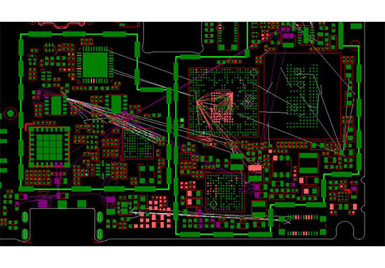
Plenty of people probably do not know the difference between high-end PCB and common PCB? Because there is not much difference in appearance;
However, if a hardware engineer is new to layout multilayer PCBs who will be easy to get dizzy. There are 8 or 10 layers in hig-end PCBs, and the traces look like spider webs.
Here share several internal structure diagrams of multi-layer Printed Circuit Boards (PCB), and used three-dimensional graphics to show the internal structure of PCB diagrams of various laminated structures.
The core of the high-density interconnection (HDI) PCB:Via
The circuit processing of multi-layer PCB is no different from single-layer and double-sided PCB. The biggest difference lies in the technics of vias.
The lines are all etched, and the vias are all drilled and then plated with copper. Multilayer circuit boards usually include through-hole boards, 1 stage boards, 2 stage boards, and second-level stacked-hole boards. Higher-end boards, such as s stage boards and arbitrary-layer interconnect boards, which are expensive and usually used very little;
In general, 8-bit single-chip products use 2-layer through-hole boards; 32-bit single-chip-level smart hardware uses 4-layer-6-layer through-hole boards; Linux and Android-level smart hardware uses 6-layer through-hole to 8 Stage HDI board: Compact products such as smart phones generally use 8-layer 1 Stage to 10-layer 2-Stage circuit boards.
The most common through holes
There is only one type of via, from the first layer to the last layer. Whether it is an external circuit or an internal circuit, the holes are punched through. It is called through-hole board.
Through-hole boards and the number of layers do not matter. Everyone usually uses two-layer through-hole boards, and many switches and military circuit boards design to 20-layer through-hole boards.
Use a drill to drill through the circuit board, and then plate the hole with copper to form a via.
It should be noted here that the inner diameter of the through hole is usually 0.2mm, 0.25mm and 0.3mm, but generally the 0.2mm is much more expensive than the 0.3mm. Because the drill bit is too thin and easy to break, then the drill speeding is slower. The time spent and the cost of the drill bit are reflected in the increase in the price of the circuit board.
Laser hole of High Density Interconnect(HDI) Board
This picture is a laminated structure picture of a 6-layer 1-stage HDI board. Both layers on the surface are laser holes with an inner diameter of 0.1mm. The inner layer is a mechanical hole, which is equivalent to a 4-layer through-hole board, and the outer layer is covered with 2 layers.
The laser can only penetrate glass fiber sheets, not metal copper. Therefore, the outer surface punching will not affect other internal circuits.
After the laser drills the hole, go to copper plating, and the laser via is formed.
2-Stage HDI board, 2Layer of laser holes
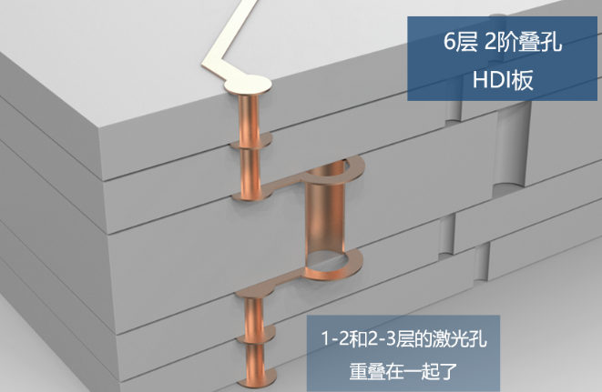
This picture is a 6-layer, 2- stage HDI board with misaligned holes. Usually, people use 6-layer, 2- stage few, and most of them start with 8-layer, 2-stage. More layers here are the same as 6 layers;
The so-called 2nd stage means there are 2 layers of laser holes;
The so-called staggered hole means that the two layers of laser holes are staggered.
Why should it be staggered? Because the copper plating is not full, the inside of the hole is empty, so you can’t drill holes directly on it, you have to stagger a certain distance, and then make a layer of empty.
6 layers of 2 stage = 4 layers of 1 stage plus 2 layers outside.
8 layers of 2 stage = 6 layers of 1 stage plus 2 layers outside.
Stacked orifice board is much more complicated technics as well as higher price.
The two layers of laser holes of the staggered hole board overlap each other. The line will be more compact.
The inner laser hole need to be electroplated and filled, and then the outer laser hole is made. The price is more expensive than the taggered hole.
Super expensive any layer interconnection board, multilayer laser stacking holes
That is, each layer is a laser hole, and each layer can be connected together. You can route the cables as you want, and punch as you want.
Therefore, only electronics products like iphone is willing to use it. For other mobile phone brands, I have never heard of anyone who has used any layer of interconnection boards.
Whether it is drawn by hand or drawn by CAD, in short, only got Schematics can start PCB Layout;
2. The circuit power consumption calculation sheet (Unnecessary)
There are data about the power supply voltage and the current flowing through every single component. Without this, you need to interpret the Schematics to design the trace width and trace spacing.
In the absence of special software, free software such as LTspice can be used for circuit simulation.
In addition, verify through written calculations, and record the voltage value, positive and negative, current value and direction of flow for the places you need to check in the future.
The application in circuit board design is to calculate the width of the trace based on the current flowing through a certain area, especially for voltage traces and GND traces so that it can be used as a basis for designing connections the size and number of holes.
3. The electrical list of the Schematics (Unnecessary)
If no electrical list of the Schematics, which is able to make by yourself in the light of the Schematics. After all, the circuit electrical list is necessary for circuit board design.
Bt the way, the electrical network list for the circuit board is divided into a circuit diagram electrical network list and a circuit board electrical network list.
In many cases, especially when the circuit board is revised, the electrical network list will not be given. At this time, you need to do it yourself.
4. Bill of Materials (BOM) (Necessary)
Here to compare the consistency of the Schematics and the BOM. And mainly two reasons causing the inconsistency:
1>Constant changing when designing new products;
2>Components are eliminated or updated when the product is revised;
Therefore, no matter how much time it takes, the Schematics must be consistent with the component list to ensure the success rate of the PCB Layout.
5. Circuit board design drawings (Necessary)
Even scribbled handwriting is still terribly necessary. If it is only delivered verbally, which will be possible lead to errors due to misunderstand the meaning of the product designer.
The content of the drawing: Board, surface treatment, the minimum limit of trace width and trace spacing, the specifications of the pads, the font and size of the printing.
The size of the circuit board, the location where the specified component is placed, and the prohibited area. Insulation specifications between different areas, etc.
6. Circuit board layout schedule
Calculate how long the circuit board layout takes, and how many layout engineers requries.
7. Circuit board area estimation table
Within the specified circuit board size, judge whether the components can be reasonably arranged in the circuit board.
In the case that the components can be arranged in the circuit board, it is judged whether to adopt a two-layer design, four-layer design or more.
Apart from that, in the absence of any designation, it is also necessary to fully communicate with the product designer to recommend the most appropriate circuit board size and layer design.
8. Workpiece size estimation table
After determining the size of the circuit board, in order to achieve the minimum production cost in production, several individual circuit boards will be connected together by V-cutting. At this time, the appropriate workpiece size must be selected.
9. Circuit board electrical design table
It includes the following parts:
1>Trace width calculation table or trace width reference table;
2>Trace spacing calculation table or trace spacing reference table;
Pad, the basic unit of surface mount assembly, which is used to form the land pattern of the printed circuit board (PCB). That’s to say, a variety of land combinations designed for special component types. The pad is used for electrical connection, device fixing, or part of the conductive pattern that combines both.
Types of pads in PCB design
1. Common pads
1>Square pads–Frequently used when the printed circuit board components are large and less as well as the printed traces are simple. Therefore, using this type of pads will be easy if make a PCB by hand.
2>Circular pads–Widely used in single and double-sided printed circuit boards whose components are regularly arrayed. If the density of the board allows, the pads can be designed larger so that the components will not fall off during soldering.
3>Island-shaped pads–The connection between the pads is integrated. It is often used in vertical irregular array placement.
4> Polygonal pads–Be used to distinguish pads with close outer diameters but different apertures, which is convenient for assembly.
5>Oval pads–With enough area to enhance the anti-stripping ability, it is often used in dual in-line components.
6>Open-shaped pads–In order to ensure manually repaired pads holes are not sealed by solder after wave soldering;
2. Special pads
1> Plum blossom pad
Plum blossom pads are usually used in large vias to ground. Here are a couple of reasons why require such design:
1) The fixing hole need to be metallized and connected to GND. If the fixing hole is fully metallized, then which is easy to block the hole during reflow soldering.
2) The use of internal metal screw holes may cause the grounding to be in a poor state due to installation or multiple disassembly and assembly. However, using plum blossom pads can ensure a good grounding regardless of the tweaks in the stress.
2> Cross-shaped pad
Cross-shaped pads are also called thermal pads, hot air pads, and so on. Its function is to reduce the heat dissipation of the pads during soldering, so as to prevent false soldering or PCB peeling caused by excessive heat dissipation.
1) When the pad is ground. The cross-shaped pad pattern can reduce the area of the ground wire, slow down the heat dissipation speed and facilitate welding.
2) When the PCB requires machine placement, and it is a reflow soldering machine, the cross-shaped pad can prevent the PCB from peeling (because more heat is needed to melt the solder paste).
3>Teardrop-shape pad
It is often used when the traces connected to the pads are thin, and teardrop shape pads are effectively able to prevent the pads from peeling and the traces are disconnected from the pads. Such teardrop-shape pads are commonly used in high-frequency circuits.
PCB design impedance matching refers to a suitable matching method between the signal source or transmission line and the load. According to the access method, the impedance matching of PCB design has two methods: Serial and parallel; And in the light of the frequency of the signal source, the impedance matching of PCB design can be divided into another two types:Low frequency and high frequency.
High frequency signals generally use serial PCB design impedance matching
The resistance value of the series resistor is 20~75Ω, and the resistance value is proportional to the signal frequency and inversely proportional to the PCB trace width. In embedded systems, serial matching resistors are generally required for signals with frequencies greater than 20M and PCB trace lengths greater than 5cm, such as clock signals, data and address bus signals in the system. There are two functions of series matching resistance:
1> Reduce high frequency noise and edge overshoot. If the edge of a signal is very steep, it contains a lot of high-frequency components, which will radiate interference. In addition, it is also prone to overshoot. The series resistance and the distributed capacitance of the signal line and the load input capacitance form an RC circuit, which will reduce the steepness of the signal edge.
2> Reduce high frequency reflection and self-excited oscillation. When the frequency of the signal is high, the wavelength of the signal is very short. However, if the wavelength is as short as the length of the transmission line, the reflected signal superimposed on the original signal will change the shape of the original signal. If the characteristic impedance of the transmission line is not equal to the load impedance (that is, it does not match), reflections will occur at the load end, causing self-oscillation. The low-frequency signal of the wiring in the PCB board can be directly connected, and generally no serial matching resistor is required.
Parallel PCB design impedance matching is also called “terminal PCB design impedance matching”
Generally used in the input/output interface, which mainly refers to the impedance matching with the PCB design of the transmission cable. For example, LVDS and RS422/485 use Category 5 twisted-pair cables with input end matching resistance of 100~120Ω; Video signals use coaxial cables with matching resistance of 75Ω or 50Ω, and flat cables with a matching resistance of 300Ω. The resistance value of the parallel matching resistor is related to the medium of the transmission cable and has nothing to do with the length. Its main function is to prevent signal reflection and reduce self-excited oscillation.
It is worth mentioning that the impedance matching of PCB design can improve the EMI performance of the system. In addition, in order to solve the impedance matching of PCB design, in addition to using series/parallel resistors, transformers can also be used for impedance transformation. Typical examples are Ethernet interfaces and CAN buses.
2. Zero ohm resistance
1> The easiest way is to use it as a jumper. If a certain section of the circuit is not used, just do not solder the resistor directly (it will not affect the appearance).
2>When the matching circuit parameters are uncertain, replace them with zero ohms. In actual debugging, determine the parameters and replace them with specific numerical components.
3> When you want to measure the working current of a certain part of the circuit, you can remove the zero-ohm resistance and connect an ammeter to facilitate current measurement.
4> In the PCB design and layout, if the layout is really impossible, you can also add a zero ohm resistor to act as a jumper.
5> In the high-frequency signal network, it acts as an inductor or a capacitor (for PCB design impedance matching, zero-ohm resistance also has impedance). When used as an inductor, it mainly solves the EMC problem.
6> Single-point grounding, such as the single-point connection of analog ground and digital ground.
7> The configuration circuit can replace jumpers and DIP switches. Sometimes users will change the settings randomly, which is easy to cause misunderstanding. In order to reduce maintenance costs, zero-ohm resistors are used instead of jumper wires to be soldered on the board.
8> For system debugging, for example, divide the system into several modules, and separate the power supply and ground between the modules with a zero-ohm resistance. When the power supply or ground is short-circuited during the debugging stage, removing the zero-ohm resistance can narrow the search range.
The above functions can also be replaced by “magnetic beads”. Although zero-ohm resistance and magnetic beads are somewhat similar in function, there are essential differences. The former has an impedance characteristic, and the latter has an inductive reactance characteristic. Magnetic beads are generally used in power and ground networks for filtering.
1. If the designed circuit system includes FPGA devices, the Quartus II software must be used to verify the pin assignments before drawing the Schematic. (Some special pins in FPGA cannot be used as ordinary IO).
2. 4-layer board from top to bottom is signal plane layer, ground, power, signal plane layer; While 6-layer board from top to bottom that is signal plane layer, ground, signal inner electric layer, signal inner electric layer, power and signal plane layer. For boards with 6 layers and above (the advantage is: anti-interference radiation), the internal electrical layer wiring is preferred, and the plane layer is not allowed to go. It is forbidden to wire from the ground or power layer ( Mainly considering the power layer will be divided, causing parasitic effects).
3. Routing of multi-power system: If FPGA+DSP system is made of 6-layer board, there will be at least 3.3V+1.2V+1.8V+5V.
3.3V is generally the main power supply, and the power layer is directly laid, and which is easy to route the global power network through the vias;
5V may generally be the power input, and only a small area of copper is required. And as thick as possible.
1.2V and 1.8V are the core power supply (if you directly use the wire connection method, you will encounter great difficulties when facing BGA devices). Try to separate 1.2V and 1.8V during layout, and let 1.2V or 1.8V connect The components are arranged in a compact area and connected by copper
In short, because the power supply network is spread over the entire PCB, it will be very complicated and long to go around if you use the wiring method. At this time, the method of laying copper is a good choice!
4. The routing between adjacent layers adopts a cross method: It is able to reduce electromagnetic interference between parallel wires and facilitate routing.
5. What is the isolation method for analog and digital isolation? Separate the devices used for analog signals and digital signals during layout, and then cut across the AD chip!
The analog signal is laid with an analog ground, and the analog ground/analog power supply and the digital power supply are connected at a single point through an inductor/magnetic bead.
6. PCB design based on PCB design software can also be regarded as a software development process. Software engineering pays most attention to the idea of ”iterative development” to reduce the probability of PCB errors.
(1) Check the schematic diagram, pay special attention to the power and ground of the device (power and ground are the blood of the system, and there can be no negligence);
(2) PCB package drawing (confirm whether the pins in the schematic diagram are wrong);
(3) After confirming the PCB package size one by one, add a verification label and add it to the package library of this design;
(4) Import the netlist and adjust the signal sequence in the schematic while layout (OrCAD component automatic numbering function can no longer be used after layout).
In the specific PCB design process, the basic knowledge that need to be mastered includes:
1. Preliminary Preparation
Including the preparation of component libraries and Schematic. Before proceeding with PCB design, we must first prepare the schematic SCH component library and PCB component packaging library.
The PCB component package library is best established by the engineer based on the standard size data of the selected device. In principle, establish the PC component package library first, and then establish the schematic SCH component library.
PCB component packaging library requirements are high, it directly affects the installation of PCB; schematic SCH component library requirements are relatively loose, but pay attention to define the pin attributes and the corresponding relationship with the PCB component packaging library.
2. PCB Structure Design
According to the determined circuit board size and various mechanical positioning, draw the PCB frame in the PCB design environment, and place the required connectors, buttons/switches, screw holes, assembly holes, etc. according to the positioning requirements.
Fully consider and determine the wiring area and non-wiring area (such as how much area around the screw hole belongs to the non-wiring area).
3. PCB Layout
PCB Layout is to place the devices in the PCB frame according to the design requirements. Generate the netlist (Design→CreateNetlist) in the schematic tool, and then import the netlist (Design→ImportNetlist) in the PCB software. After the netlist is successfully imported, it will exist in the background of the software. Through the Placement operation, all devices can be called out, and there is a flying line prompt connection between the pins. At this time, the layout design of the device can be carried out.
PCB layout is the first important process in the entire PCB design process. The more complex the PCB board, the better the layout can directly affect the difficulty of later wiring.
The layout design relies on the circuit board designer’s basic circuit knowledge and rich design experience, which is a higher level requirement for the circuit board designer. The junior circuit board designer has little experience and is suitable for small module layout design or PCB layout tasks with lower difficulty of the whole board.
4. PCB Routing
PCB routing is the process with the largest workload in the whole PCB design, which directly affects the performance of PCB board.
In the PCB design process, there are three various levels about PCB routing:
>Routing reasonably, which is the most basic entry requirement for PCB design;
>The satisfaction of electrical performance, which is a standard to measure whether a PCB board is qualified. After the Layout is initially finished, carefully adjust the routing to achieve the best electrical performance;
>Neat and beautiful PCB Layout. Messy routing, even if the electrical performance is passed, it will still bring extremely inconvenience to the optimization of the later board modification, testing and maintenance. Therefore, for PCB Layout, routing always require neat and uniform instead of criss-cross and disorderly.
5. Routing Optimization & Silk Screen Placement
“PCB design never be the best, only better”, “PCB design is an art of defects”, this is mainly because PCB design need to realize the design requirements of all aspects of hardware, and individual requirements may be in conflict.
For instance, a PCB design project need to be designed as a 6-layer board after evaluation by the circuit board designer; However, the product hardware must be designed as a 4-layer board due to cost considerations, so the signal shielding ground layer can only be sacrificed, resulting in adjacent routing whose signal crosstalk between layers increases but signal quality decreases.
The general design experience is: Time in optimizing routing is twice of the first routing. After the PCB layout optimization is completed, post-processing is required. The first thing to do is the silk screen logo on the PCB surface. Also, the bottom silk screen letters need to be mirrored during design to avoid confusion with the top silk screen.
6. Network DRC Inspection & Structure Inspection
Quality control is an important part during PCB design process. General quality control methods include: Self-inspection, mutual inspection, expert review meetings, special inspections, etc.
Schematic and structural element diagrams are the most basic design requirements. Network DRC inspection and structural inspection are to confirm that the PCB design meets the two input conditions of the schematic netlist and structural element diagram.
Generally, circuit board designers will have their own accumulated design quality inspection checklist, in which some items come from the company or department’s specifications, and the other part comes from their own experience summaries. Special inspections include Valor inspection and DFM inspection of the design. These two parts focus on the PCB design output back-end processing gerber file.
7. PCB Manufacturing
Before PCB is formally manufactured, the circuit board designer need to communicate with the PE of the PCB supplier and answer the manufacturer’s confirmation questions about PCB manufacturing. (EQ Confirmation Stage, EQ-Engineer Questions)
It includes but not limited: Choice of PCB board model, adjustment of circuit layer line width and line spacing, adjustment of impedance control, adjustment of PCB stacking thickness, surface treatment processing technology, aperture tolerance control and delivery standards, etc.
As we all know, a good PCB design engineer should master a wide range of knowledge systems, including electrical theory, component performance, digital and analog circuits, PCBA processing technology and DFM manufacturability theory, welding practice operations, schematic drawing and layout, and single-chip microcomputer programs Logic and basic principles, etc. In other words,
1. If the designed circuit system includes FPGA devices, the Quartus II software must be used to verify the pin assignments before drawing the Schematic. (Some special pins in FPGA cannot be used as ordinary IO).
2. 4-layer board from top to bottom is signal plane layer, ground, power, signal plane layer; While 6-layer board from top to bottom that is signal plane layer, ground, signal inner electric layer, signal inner electric layer, power and signal plane layer. For boards with 6 layers and above (the advantage is: anti-interference radiation), the internal electrical layer wiring is preferred, and the plane layer is not allowed to go. It is forbidden to wire from the ground or power layer ( Mainly considering the power layer will be divided, causing parasitic effects).
3. Routing of multi-power system: If FPGA+DSP system is made of 6-layer board, there will be at least 3.3V+1.2V+1.8V+5V.
3.3V is generally the main power supply, and the power layer is directly laid, and which is easy to route the global power network through the vias;
5V may generally be the power input, and only a small area of copper is required. And as thick as possible.
1.2V and 1.8V are the core power supply (if you directly use the wire connection method, you will encounter great difficulties when facing BGA devices). Try to separate 1.2V and 1.8V during layout, and let 1.2V or 1.8V connect The components are arranged in a compact area and connected by copper
In short, because the power supply network is spread over the entire PCB, it will be very complicated and long to go around if you use the wiring method. At this time, the method of laying copper is a good choice!
4. The routing between adjacent layers adopts a cross method: It is able to reduce electromagnetic interference between parallel wires and facilitate routing.
5. What is the isolation method for analog and digital isolation? Separate the devices used for analog signals and digital signals during layout, and then cut across the AD chip!
The analog signal is laid with an analog ground, and the analog ground/analog power supply and the digital power supply are connected at a single point through an inductor/magnetic bead.
6. PCB design based on PCB design software can also be regarded as a software development process. Software engineering pays most attention to the idea of ”iterative development” to reduce the probability of PCB errors.
(1) Check the schematic diagram, pay special attention to the power and ground of the device (power and ground are the blood of the system, and there can be no negligence);
(2) PCB package drawing (confirm whether the pins in the schematic diagram are wrong);
(3) After confirming the PCB package size one by one, add a verification label and add it to the package library of this design;
(4) Import the netlist and adjust the signal sequence in the schematic while layout (OrCAD component automatic numbering function can no longer be used after layout).
In the specific PCB design process, the basic knowledge that need to be mastered includes:
1. Preliminary Preparation
Including the preparation of component libraries and Schematic. Before proceeding with PCB design, we must first prepare the schematic SCH component library and PCB component packaging library.
The PCB component package library is best established by the engineer based on the standard size data of the selected device. In principle, establish the PC component package library first, and then establish the schematic SCH component library.
PCB component packaging library requirements are high, it directly affects the installation of PCB; schematic SCH component library requirements are relatively loose, but pay attention to define the pin attributes and the corresponding relationship with the PCB component packaging library.
2. PCB Structure Design
According to the determined circuit board size and various mechanical positioning, draw the PCB frame in the PCB design environment, and place the required connectors, buttons/switches, screw holes, assembly holes, etc. according to the positioning requirements.
Fully consider and determine the wiring area and non-wiring area (such as how much area around the screw hole belongs to the non-wiring area).
3. PCB Layout
PCB Layout is to place the devices in the PCB frame according to the design requirements. Generate the netlist (Design→CreateNetlist) in the schematic tool, and then import the netlist (Design→ImportNetlist) in the PCB software. After the netlist is successfully imported, it will exist in the background of the software. Through the Placement operation, all devices can be called out, and there is a flying line prompt connection between the pins. At this time, the layout design of the device can be carried out.
PCB layout is the first important process in the entire PCB design process. The more complex the PCB board, the better the layout can directly affect the difficulty of later wiring.
The layout design relies on the circuit board designer’s basic circuit knowledge and rich design experience, which is a higher level requirement for the circuit board designer. The junior circuit board designer has little experience and is suitable for small module layout design or PCB layout tasks with lower difficulty of the whole board.
4. PCB Routing
PCB routing is the process with the largest workload in the whole PCB design, which directly affects the performance of PCB board.
In the PCB design process, there are three various levels about PCB routing:
>Routing reasonably, which is the most basic entry requirement for PCB design;
>The satisfaction of electrical performance, which is a standard to measure whether a PCB board is qualified. After the Layout is initially finished, carefully adjust the routing to achieve the best electrical performance;
>Neat and beautiful PCB Layout. Messy routing, even if the electrical performance is passed, it will still bring extremely inconvenience to the optimization of the later board modification, testing and maintenance. Therefore, for PCB Layout, routing always require neat and uniform instead of criss-cross and disorderly.
5. Routing Optimization & Silk Screen Placement
“PCB design never be the best, only better”, “PCB design is an art of defects”, this is mainly because PCB design need to realize the design requirements of all aspects of hardware, and individual requirements may be in conflict.
For instance, a PCB design project need to be designed as a 6-layer board after evaluation by the circuit board designer; However, the product hardware must be designed as a 4-layer board due to cost considerations, so the signal shielding ground layer can only be sacrificed, resulting in adjacent routing whose signal crosstalk between layers increases but signal quality decreases.
The general design experience is: Time in optimizing routing is twice of the first routing. After the PCB layout optimization is completed, post-processing is required. The first thing to do is the silk screen logo on the PCB surface. Also, the bottom silk screen letters need to be mirrored during design to avoid confusion with the top silk screen.
6. Network DRC Inspection & Structure Inspection
Quality control is an important part during PCB design process. General quality control methods include: Self-inspection, mutual inspection, expert review meetings, special inspections, etc.
Schematic and structural element diagrams are the most basic design requirements. Network DRC inspection and structural inspection are to confirm that the PCB design meets the two input conditions of the schematic netlist and structural element diagram.
Generally, circuit board designers will have their own accumulated design quality inspection checklist, in which some items come from the company or department’s specifications, and the other part comes from their own experience summaries. Special inspections include Valor inspection and DFM inspection of the design. These two parts focus on the PCB design output back-end processing gerber file.
7. PCB Manufacturing
Before PCB is formally manufactured, the circuit board designer need to communicate with the PE of the PCB supplier and answer the manufacturer’s confirmation questions about PCB manufacturing. (EQ Confirmation Stage, EQ-Engineer Questions)
It includes but not limited: Choice of PCB board model, adjustment of circuit layer line width and line spacing, adjustment of impedance control, adjustment of PCB stacking thickness, surface treatment processing technology, aperture tolerance control and delivery standards, etc.