The transmission rate of high-speed PCB design and routing system is accelerating with the changes of the times, but which also brings a new challenge to it – The anti-interference ability is getting weaker and weaker. This all stems from the fact that the higher the frequency of information transmission, the more sensitive the signal and the weaker the energy, so the routing system is more and more susceptible to interference. In some common electronic equipment, such as computer screens, mobile phones, motors, radio broadcasting equipment, etc., cables and equipment are able to interfere with other components or be seriously interfered by other interference sources.
Shielding Methods In High Frequency PCB Design
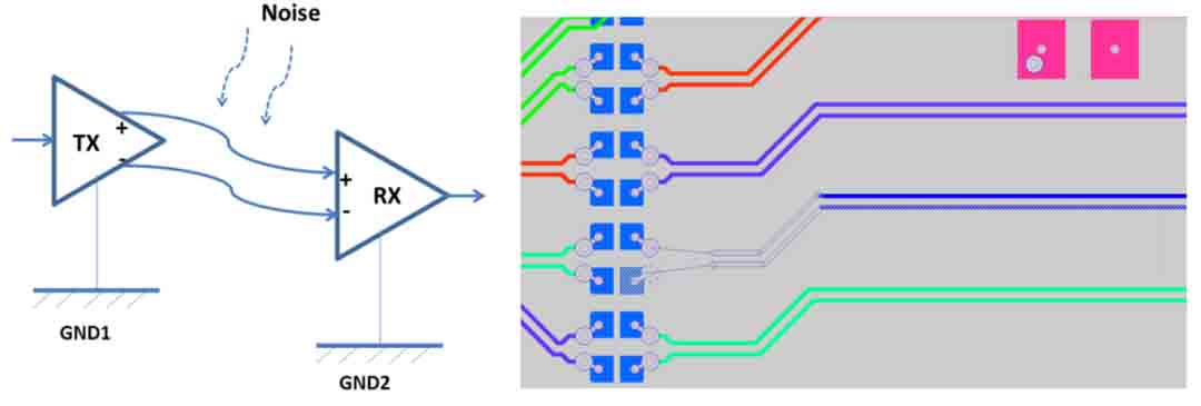
Especially when using high-speed data networks, the time required to intercept a large amount of information is significantly lower than the time required to intercept low-speed data transmissions. The twisted pair in the data twisted pair can resist external interference and inter-pair crosstalk through its own twisting at low frequencies, but at high frequencies (especially when the frequency exceeds 250MHz), the twisting alone cannot achieve anti-interference. Purpose, only shielding can resist external interference.
The cable shield acts like a Faraday shield. Interfering signals enter the shield, but not the conductors. Therefore, the data transfer can operate without problems. Network transmission is blocked because shielded cables have lower radiated emissions than unshielded cables. Shielded networks (shielded cables and components) can significantly reduce the radiation level of electromagnetic energy that may be intercepted as it enters the surrounding environment.
Shielding options for different interference fields mainly include electromagnetic interference and radio frequency interference. Electromagnetic interference (EMI) is mainly low frequency interference. Electric motors, fluorescent lamps, and power lines are common sources of EMI. Radio frequency interference (RFI) refers to radio frequency interference, mainly high frequency interference. Wireless communications such as radio, television broadcasting, and radar are common sources of RF interference. For immunity to EMI, braided shielding is the most effective because of its lower critical resistance; For RFI, foil shielding is the most effective. Since the braided shielding depends on the change of wavelength, the gap generated by the braided shield allows the high-frequency signal to freely enter and exit the conductor; for the mixed interference field of high and low frequencies, the combined shielding method of the foil layer with the broadband coverage function and the braided mesh should be adopted. Generally speaking, the higher the mesh shielding coverage, the better the shielding effect.
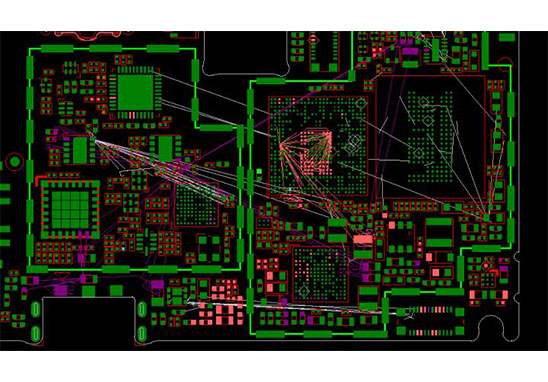
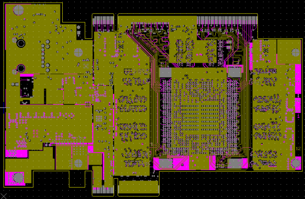
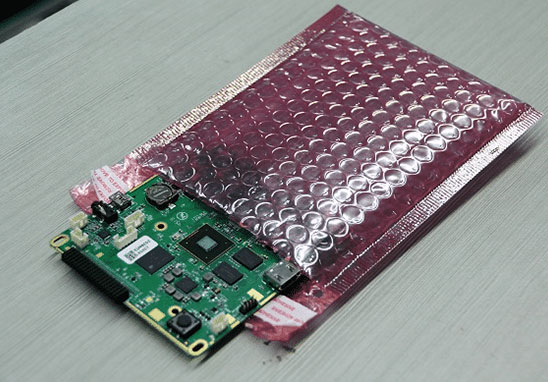
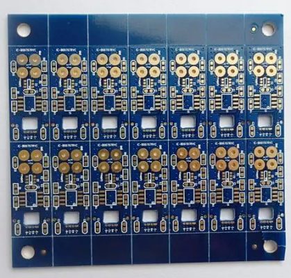
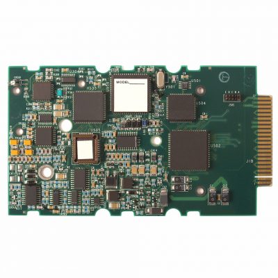
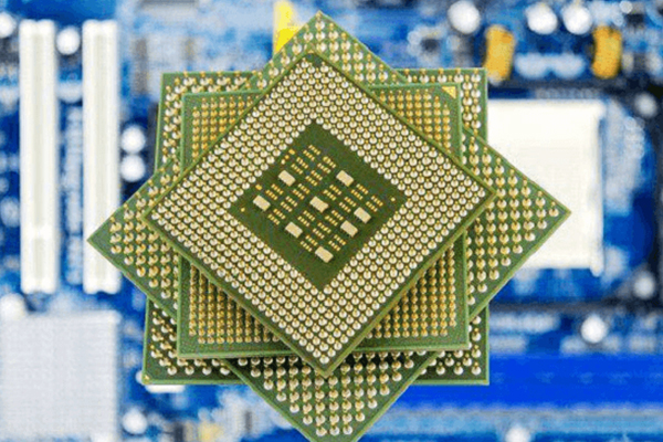
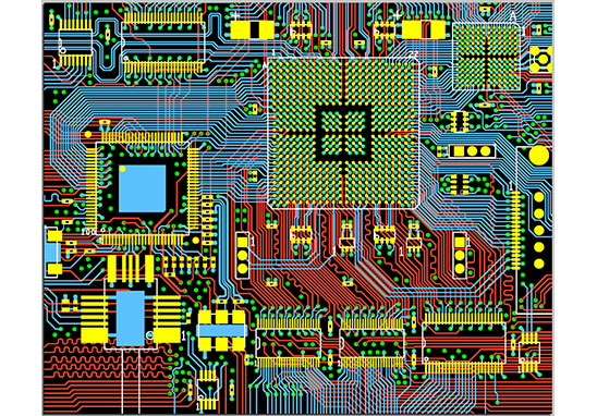
Grande’s PCB Design Capabilities
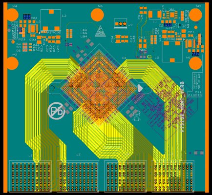
Maximum Signal Design Rate: 10Gbps CML differential signal;
Maximum PCB Layout Layers: 40 layers;
Minimum Line Width: 2.4mil;
Minimum Line Spacing: 2.4mil;
Minimum BGA PIN Spacing: 0.4mm;
Minimum Mechanical Hole Diameter: 6mil;
Minimum Laser Drilling Diameter: 4mil;
Maximum Number of PINs: ;63000+
Maximum Number of Components: 3600;
Maximum Number of BGAs: 48+.

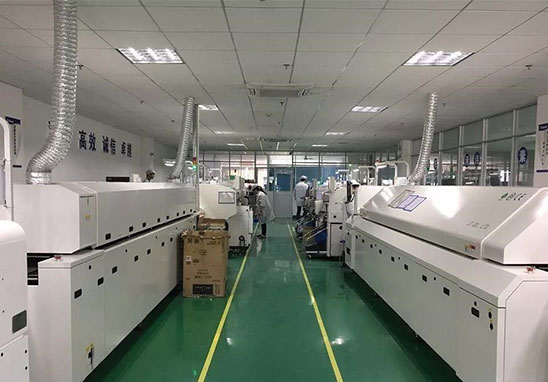
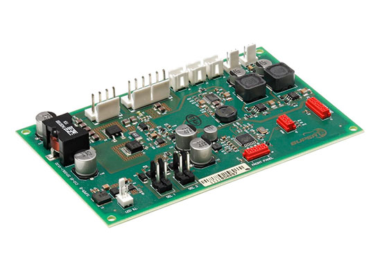
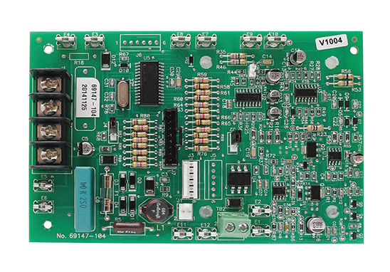
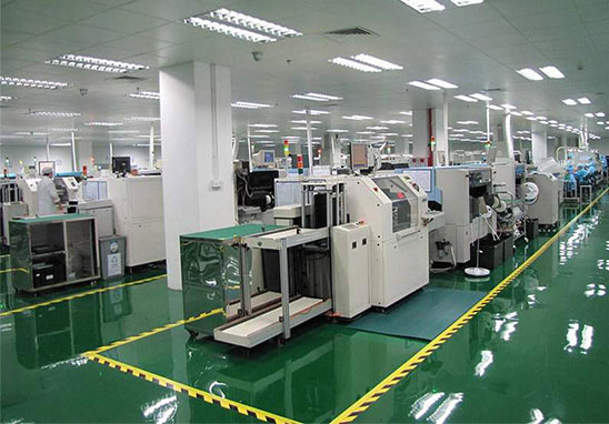
Advantages Grande Circuit Board Assembly
1)Strength Guarantee
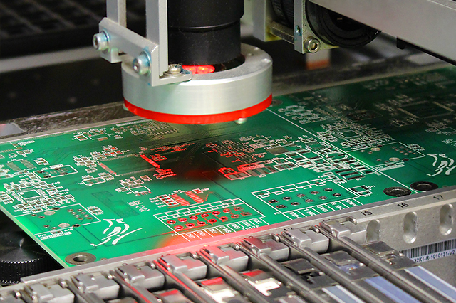
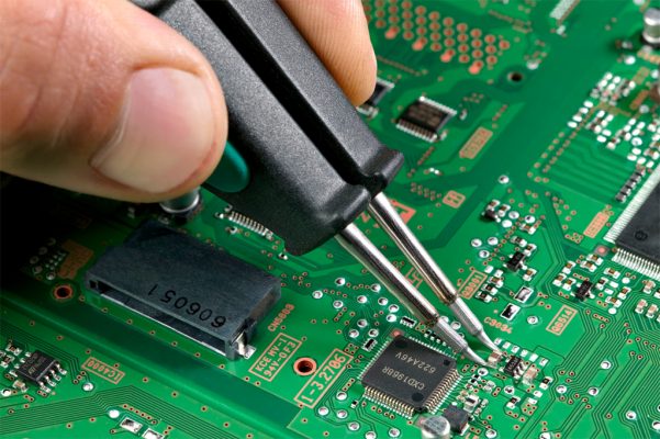
▪ SMT factory: With imported SMT machines and multiple optical inspection equipment, which is able to produce 4 million points per day. Each process is equipped with QC personnel who will keep an eye on product quality.
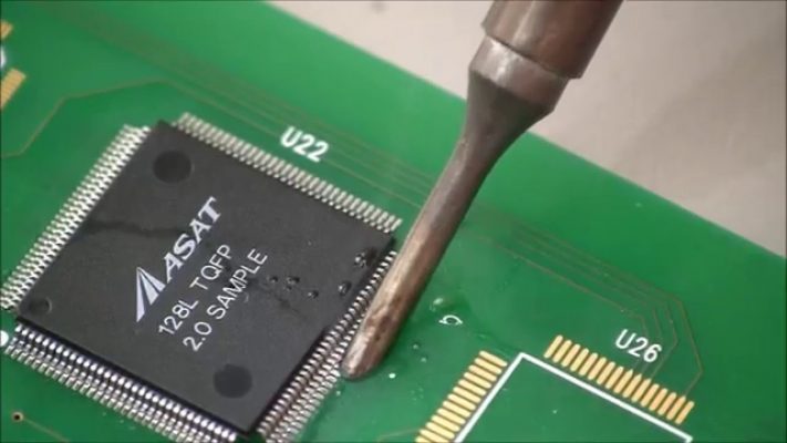
▪ DIP production line: Two wave soldering machines and more than 10 employees who have worked for over three years. That’ s to say, these workers are highly skilled and can weld various SMT & DIP components.
2)Quality Assurance With High Cost Performance
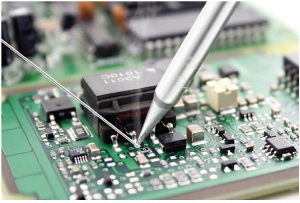
▪ High-end equipment can paste precision special-shaped parts, BGA, QFN, 0201 package. It can also be soldered prototype PCBA via SMT machine and placing bulk materials by hand.
▪ Both samples, small and large batches can be produced. And there is no SMT Machine starting cost.
3)Rich Electronic Products SMT Soldering Experience With Stable Delivery
▪ Accumulated services to thousands of electronics companies, involving SMT soldering services for various types of automotive equipment and industrial control motherboards. Furthermore, PCBA Products are often exported to Europe and the United States, and the quality is able to be affirmed by new and regular customers.
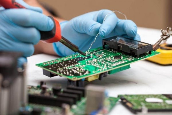
4)Strong Maintenance Ability & Reliable After-Sales Service
▪ The maintenance engineers have sophisticated experience so that those defective boards caused by all kinds of SMT soldering can be repaired. Meanwhile, ensuring the connectivity rate of each circuit board also make sense.
▪Order problems feedback will get response, solution and solved as soon as possible.