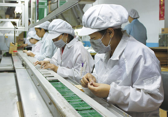
About PCBA welding process, there are many requirements for the PCBA .It must meet the requirements in order to weld.
Then why does the welding process have so many requirements for PCBA? That is because PCBA will go through many special processes in the processing. The application of special processes brings many requirements to the PCB board. If the PCB has problems, it will increase the difficulty of the PCBA soldering process. Eventually it may lead to there will be welding defects, board failure and other problems.
Therefore, in order to ensure the smooth completion of the special process, and also for the PCBA can be more easily welding. The size of the PCB board, the distance between the pads, etc. should meet the manufacturability requirements. Next, GrandePCBA will take you to see the PCBA requirements for PCB processing.

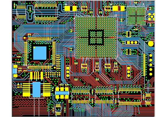
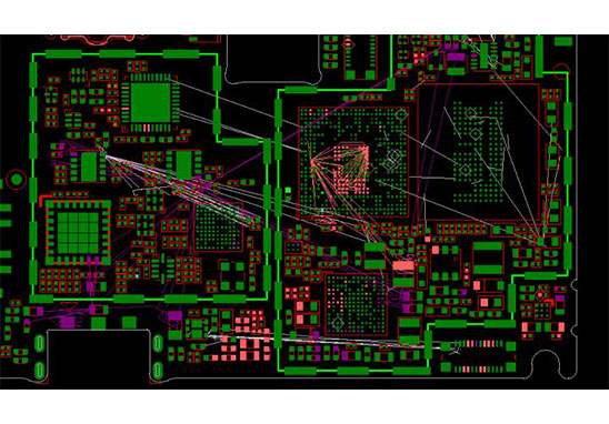
PCBA soldering requirements for PCB boards
1.PCB size
PCB width (including board edge) should be greater than 500mm, less than 460mm
PCB length (including board edge) should be greater than 500mm
If size is too small, you need to do the panel.
2.PCB board edge width
Board edge width: >5mm, the panel spacing: 8mm, the distance between the pad and the board: >5mm
3.PCB curvature
Board edge width: >5mm, panel spacing: 8mm, the distance between the pad and the board: >5mm
4.PCB board Mark point
Mark point shape: standard circle, square, triangle.
Mark point size; 0.8~1.5mm.
Mark point material: gold-plated, tin-plated, copper-platinum.
Mark point surface requirements: smooth surface, no oxidation, no dirt
Other requirements of the Mark point: there shall be no green or other obstacles within 1mm around, which is obviously different from the Mark point color;
Mark point position: more than 3mm away from the edge,and no mark point vias, test points, etc. within 5mm around.
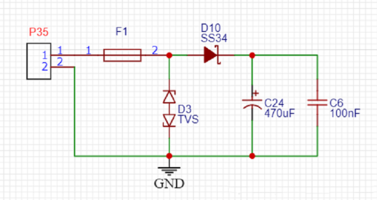
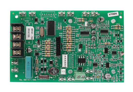
5.PCB pads
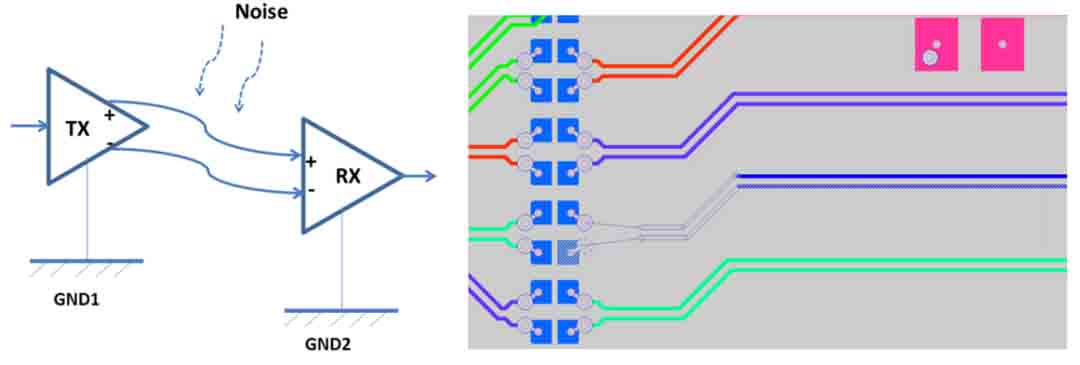
SMD components cannot have through-holes on the pads. The through hole will allow the solder paste to flow into the hole, resulting in less tin in the parts, or the tin flow to the other side, resulting in uneven board surface, and the solder paste cannot be printed
When doing PCB design and production, it is necessary to understand some knowledge of PCBA soldering process to make the product suitable for production. Understanding the requirements of the PCBA processing plant first can make the subsequent manufacturing process smoother and avoid unnecessary troubles.

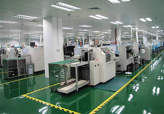
About Grande
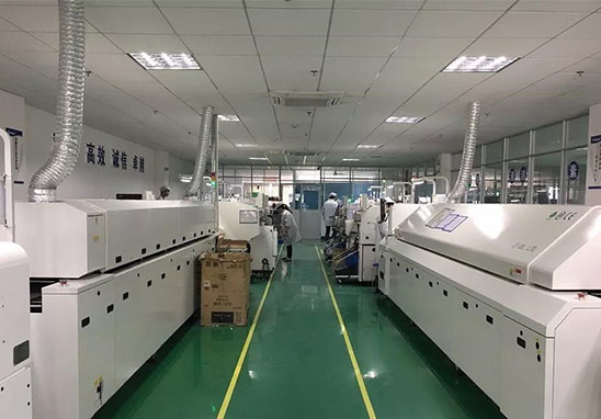
Grande specializes in providing overall PCBA electronic manufacturing services, including electronic components procurement to PCB production and processing, SMT patch, DIP plug-in, PCBA testing, finished product assembly .Turnkey one-stop PCBA services.
The company gives full play to its competitive advantages in scale procurement and quality control, and signs long-term cooperation agreements with many electronic component manufacturers at home and abroad to ensure the quality and stable supply of raw material sources, and transfer the preferential treatment to customers.
Maintaining the purchasing advantages of IC, resistors, capacitors, inductors, transistors and other components for a long time can greatly save customers’ inventory costs, improve production turnover efficiency and save time. At present, we provide PCBA processing services for customers in the United States, the United Kingdom, Japan, Russia, France, Canada, Australia, Romania, Switzerland and other countries and regions.